THE BLOG

12
Sep

Headphone amplifier – RJM Sapphire v4.2

The story of this amplifier began with the need to trade my beloved Hifiman Arya Stealth for closed-backs because I only use headphones when I am in the office and open-back headphones are disturbing others.I found a trade deal for ZMF Atticus with Eikon pad and I traded without even listening to them. As expected, they sound much less exciting than the Arya Stealth but they still sound good for closed-back headphones.

However, as their impedance is 300 ohms, I needed something more powerful than my portable Cayin RU-6 and the integrated amplifier in my Topping DX3 Pro. I had the RJM Sapphire v4.2 boards laying around from a group buy and also a Modu Shop enclosure I bought a while ago that was just the right size for this build.

The documentation in the RJM website is very informative and contains a detailed BOM file that includes formulas and example values for different gain values. If you still have some questions you can also search by keyword in the DIYAudio topic, which also has a lot of info.

RJM Sapphire v4.2 schematic

I opted out for the open loop configuration with a 21 fixed gain as I will be using it with only one pair of headphones so far. That’s why JP1, R2B, R2C, R3X are not installed on the board. You can find info on those in the BOM file.

This photo was taken in the middle of soldering the components to the boards. Resistors are different types in the different positions, of course they are consistent between right and left channel board, just because that’s what I had in my parts bin.

RJM Sapphire v4.2 PCBs

The trickiest part of amplifier building, drilling the enclosure, front and back panels. I am getting better and quicker with each amplifier and of course with all the mistakes I made in the past.

Front and back pannels drilled

In the next photos the amplifier is 99% ready and already tested with a cheap pair of headphones for stability, oscillations and temperature issues in any of the transistors.

DIY RJM Sapphire Headphone Amplifier Build Inside

Without matching any of the transistors or even measuring their hfe at all I was able to adjust the output DC to values within +-10mV which is good enough for unmatched parts.

DIY RJM Sapphire Headphone Amplifier Build Inside 2

I forgot to take one more photos when I earthed the chassis, the output and the potentiometer, but just to remind you if you are building it – always take care of your grounding.

I will also make sure to upload more photos when I 3D print a volume knob and close the lid.

As I expected, a more powerful amplifier was definitely needed with the ZMF Atticus, they sound much meatier and with better control with more power from the RJM Sapphire.

15
Jan

First shot at class D with Hypex

After making more than 5 different DIY amplifiers in class AB I decided to try class D. After spending some time reading threads in diyaudio, audiosciencereview and asking in our local forum about what are the best class D modules I had to choose between Purifi, Hypex UcG, Hypex Ncore, ICEPower and a few others. Purifi 1ET400 has the best specs according to the datasheet but it is priced at around 600EUR for stereo set even without a SMPS. I didn’t feel like spending 900-1000EUR for a DIY amplifier just to hear what class D has to offer. There is a chance I won’t like class D sound at all. Seems that Hypex Ncore is a middle ground in high end class D modules, placed somewhere between Hypex UcG and Purifi according to several forum members.

I was initially aiming at NC252MP which is 2x250W@4R and MP means that it has integrated SMPS on the same board. Class D is all about high efficiency so why not spend a few more bucks and go for the NC502MP instead? It is rated at 2x500W at 4R and 2x350W at 8R which seems like a good match for my low sensitivity ATC speakers. I found a brand new NC502MP online so I ordered it. Keep in mind that you can’t buy NC252/502 from Hypex directly because they are OEM only, you can only buy NC400 and UcG series from their website diyclassd as a non-OEM customer. However, from time to time NC252/502MP boards appear on ebay so just look there.

The measurements of the amplifier look very promising, especially the THD. THD+N vs power plot for NC502MP:
THD+N vs power Hypex NC502MP

Here is the full datasheet of Hypex NC502MP.

While waiting for it to be shipped I designed a small “interface” board to fit the balanced(XLR) and single ended(RCA) inputs, relays to switch between them and also route some connections to allow for an external board to monitor and control the Hypex amplifier. I will probably use an Arduino based board which will monitor clipping indicator, temperature and current sense which are all available on the NC502MP 16pin connector.

Hypex Ncore input board

It hosts 2x Neutrik NC3-FAH0 XLR connectors, two RCA connectors (also Neutrik) and 100nF/100R RC network for the single ended inputs as recommended by Hypex in their great XLR pin1 grounding guide which relates to every amplifier with an XLR input too.

SE/balanced input selector

The enclosure of choice is once again from my friend Gianluca at Modushop(HiFi2000). They sent me a black front panel instead of the silver ones I use for my other amplifiers but I didn’t even bother to return it because I love how it looks.

Here are some photos of how it turned out. I still have to figure out the control board but the amplifier works without it with the inputs defaulted to XLR because that’s what I connected to normally closed contacts of the relay.

DIY Hypex NC502MP amplifier front
DIY Hypex NC502MP amplifier rear
DIY Hypex NC502MP amplifier inside

I still have to let it run for at least 20 hours before sharing my opinion on how it sounds compared to my best sounding class AB amplifier.

Once I’m ready with the control board I will update this post.

11
Jan

DIY Class AB Amplifier – Apex A40

After listening to the PeeCeeBee V4H for a while I decided it is time to finally blow the dust out of my soldering iron and take a new challenge. In our local DIY audio forum an interesting schematic started a very enthusiastic discussion and a few members swore that it sounded amazing. The schematic was called “A40” and it was created by Mile Slavković (Apex Audio), a neighbour from Serbia. Our community members did modify it a little and my friend Hristo Elefterov created a really good PCB design for it because the one that was kindly shared on DIYAudio had some design flaws especially with grounding. Here is the modified schematic and PCB design:

Apex A40 Schematic
Apex A40 PCB 3D
Thanks Hristo for the work. Please drop me an email if you like to get the PCBs.

I decided to build it in dual mono configuration, that’s basically two completely separated units for each channel in one enclosure.

Transformers of choice are two great looking Breve Tufvassons 200VA 2x40VAC toroidals from TME, one for each channel. PSU boards are very trivial thus I didn’t take any close up photos of them. Each channel is supplied by a DIY PCB which consists of a 25A bridge rectifier and four 12,000uF Cornell Dubilier SLPX, two for each supply rail. Total of 96,000uF for both channels.

Another small 6VA transformer is used for the speaker protection boards and is bolted to the enclosure using a custom drawn and 3D printed stand. I love how my 3D printer allows me to make such things in less than an hour. Speaker protection boards are from Aliexpress but I did modify them. I am using two stereo boards which I have converted to mono to stick to my dual mono concept by removing one relay from each one and also upgraded the relays to high quality Panasonic relays.
Transformer for speaker protection boards, IEC inlet, fuse holder

All wiring is 4connect oxygen free copper 2×1.5mm2 and 2×2.5mm2. Input RCA jacks are Neutrik NYS367. Output terminals are Cliff TP/6. Output terminals are one of the hardest things to find nowadays. Always use good quality RCAs and output terminals in your amplifiers. Don’t buy the ones sold on Aliexpress if you don’t like your precious music distorted by a terrible choice of metal.

NB: I am not kidding. A friend was trying out to figure out a high THD of an amplifier and tried almost everything but it was still measuring bad. After a few days of experiments he found out that the conductance of the metal of the output terminals was so bad it affected the THD measurements negatively.

Bias is set at around 120mA per pair or 60mA each.

Here are a few photos from the finished amplifier:
Apex A40 boards
Apex A40 inside
Apex A40 top view
Apex A40 rear panel

Conclusion: I am not good at recreating my listening experience in words but I must say the modified Apex A40 schematic built properly in dual mono configuration raises the bar of DIY class AB amplifiers very high. +-56VDC supplies gets me 156W at 8R which is just enough to make my low sensitivity ATC speakers sound amazing.

30
Dec

Interfacing a HD44780 LCD with Raspberry Pi over I2C

I have decided to add a 16×2 LCD to my Raspberry Pi 3 based network audio player with PCM1794 DAC in order to see what is currently playing and the bitrate of the output without having to check my phone. I don’t like the number of wires that parallel LCD connection requires so I started looking for a 16×2 LCD with I2C interface which is not too expensive.

I found a very cheap 16×2 LCD on Aliexpress and even cheaper I2C backpack for it. I personally chose green foreground with black background as it looks nice in my enclosure, but there are other options too: https://www.aliexpress.com/item/1709948156.html

First test:

I decided to use LCDproc as it is a mature solution that works (almost) out of the box with HD44780 based displays over I2C, it just needs a driver and proper configuration. It is easy to control it via a telnet-like TCP protocol with Python, PHP, C++ or any other language of choice and it has many options such as managing a scrolling text, widgets, icons etc. which reduced my code to only a few lines.

My Github repository contains everything needed to pair HD44780 based LCD displays and LCDProc on Raspberry Pi via I2C. It includes installation instructions for installing on Moode or other Raspbian/Debian based OS.

  • play.php – My script to fetch currently playing song on Moode Audio and push it to the LCD via LCDProc, you can edit this one to fit your needs
  • client.php – LCDProc PHP client library by Peter Clarke (@theapi)
  • LCDd.conf – My /etc/LCDd.conf which works perfectly with the display linked above
  • hd44780.so – Driver for LCDProc HD44780 I2C displays by @wilberforce. You should copy it to /usr/lib/lcdproc/

I am running Moode Audio v6.2.1 which is based on Raspbian so it should work with any other Debian/Raspbian based OS, and most likely with Ubuntu too. I have written a small script which parses /var/local/www/currentsong.txt (a file automatically updated by Moode) and displays currently playing song/output bitrate info on the LCD. You can rewrite the script to work for any other OS, display size or purpose.

14
May

My take on the PeeCeeBee V4H amplifier

While I was browsing the DIYAudio.com forum I found a popular schematic called PeeCeeBee V4. It had a lot of positive reviews from the DIYaudio members who had already assembled it and it looked simple and easy to assemble for someone with not so much knowledge in the solid state amplifiers.

The author (Shaan) created and published a more powerful version of it called PeeCeeBee V4H which was able to push 150W into 8ohm load on +/-56V PSU, just about the right power to satisfy my somehow low sensitivity ATC SCM11 (v2/curved) speakers.

PeeCeeBee V4H schematics

Gathering the parts

I ordered PCBs from the author himself including genuine pairs of 2SK1058/2SJ162 needed for 2 channels which he shipped to me in Bulgaria. Shaan’s PCBs are of extremely good quality and visual appearance.

While I was waiting for the delivery I called Novatech Ltd to order a custom winded 40-0-40VAC @ ~550W toroid.

For the PSU I chose to use six Cornell Dubilier(CDE) SLPX 12,000uF 63V for a total of 72,000uF or 36,000uF per rail because they seem like the best bang for the buck. I bought all the capacitors used in the PSU and amplifier boards at from Stefan at Stesys.eu. All capacitors are genuine, the prices are the lowest I could find and they deliver all over the world. All other passives needed for the amplifier I have bought from Comet.bg and Farnell. All resistors are 1% or better, all small capacitors are Wima.

Assembling the boards

I decided not to waste time ordering a custom PCB but rather paint a universal PCB with black spray paint as the other PCBs are also black. Assembling the PSU board was pretty quick, it consists of a bridge rectifier, 6x 12,000uF capacitors and some snubbers.
PeeCeeBee V4H PSU painted

PeeCeeBee V4H PSU done

For the assembly of the amplifier boards the author of the schematic/PCBs provides a great instructions and there is nothing more than I can add to it to make it easier.

Here are some photos from the assembly of the amplifier boards.
PeeCeeBee V4H Assembly Step 1

PeeCeeBee V4H Assembly Step 2

The hardest thing of all the V4H assembly for me was drilling the aluminium heatsinks and tapping the holes. I have used a 2,5mm drill to make the holes and a M3 tap to make the thread. Make sure to take your time and use alcohol while drilling and tapping instead of oil. Alcohol is better for aluminium. It is nearly impossible not to break a drill or a tap when using a hand drill machine instead of a drill machine with a stand or a table drill machine. Breaking a drill or tap inside the aluminium heatsink is a very bad experience because there is no way to get it out of there without destoying the hole/thread.

Warning: REALLY, TAKE YOUR TIME WHEN DRILLING AND TAPPING! If you ruin even one hole/thread you need to redrill all other holes because the transistors are in exact positions from one another.

PeeCeeBee V4H Assembly Step 3

The last picture was with resistors needed for the setup process consisting of VAS (Voltage Amplifier Stage) biasing, offset trimming and mosfet biasing. The process is very well explained in Shaan’s instructions.

First listening tests

PeeCeeBee V4H Test Run

After a few days of settling my first impressions are that the sound is very natural and pleasant to the ears. Overall I am completely satisfied with it. I will write a more detailed review of the sound once I have something good enough to compare to in the same room/setup.

My current setup is:
Source: DIY Volumio > XMOS > PCM1794 Source
Interconnects: DIY OFC Silver Plated Interconnects
Amplifier: DIY PeeCeeBee V4H Amplifier
Speaker cable: Chord Odyssey 2
Speakers: ATC SCM 11 v2(Curved)

I will update the post with the final look of the amplifier once I finish the enclosure.

Links for PCB info/order:
https://www.diyaudio.com/forums/group-buys/317151-peeceebee-v4h-gb.html
https://www.facebook.com/shaanpeeceebee/

12
Apr

Xiaomi M365 scooter dashboard with ESP32 and 1.3 inch TFT screen

I have recently added a nice digital dashboard to my beloved M365 electric scooter. Thanks to Dani M. and the other contributors to the project I was able to make the scooter a lot smarter.

The dashboard calculates and displays daily statistics including mileage, avg. speed, time and energy used, remaining battery mileage and battery level. When you start driving the screen changes to speedometer, wattmeter and some other realtime metrics. There are a lot more screens containing battery and ESC temperatures, BMS statistics containing voltage for each cell, total battery cycles, estimated battery health percentage, pinpointing defective cells and much more.

Demo(Spanish):

Required components:

– You must join the creators’ English or Spanish chats in Telegram in order for your ESP32 serial number to be activated(it’s free):
English: https://t.me/LCDM365ESP32English
Spanish: https://t.me/LCDM365ESP32
– Download all required files (firmware, manuals, 3d printing STLs etc.):
Original
Ptodorov’s Mirror
ESP-WROOM-32 (should be the same form factor in order to fit)
1.3″ 240×240 ST7789 SPI TFT
– 1N4148 diode (I had BYV26 on hand)
– 100R and 680R resistors
– 3D printed housing, you can find .stl files in the download (I printed this with my Ender 3 printer, but if you don’t have one you can ask/pay someone to print it for you)

Flashing the firmware to the ESP32:

Before connecting anything to the ESP32 you should flash it’s firmware.

Install ESP32 1.0.0 board in your Arduino IDE from Tools > Board > Boards Manager (Warning: ESP32 1.0.1 version will not work, choose 1.0.0 from the dropdown). Install ESP32WebServer and ESPmDNS libraries by Ivan Grokhotkov via Sketch > Include Library > Manage Libraries. Connect your PC/Mac to the ESP32 using a MicroUSB cable. In Arduino IDE choose ESP32 Dev Module from the Tools > Board menu. Change the upload speed from Tools > Upload Speed to 460800.

Now open the .ino file from the M365_Loader_v12 folder and fill your home wifi ssid and password in the //WLAN Station parameters variables. Click the Upload button and wait for it to finish. Now open Tools > Serial Monitor and take a look at the log, it should connect to you home WiFi and display it’s assigned IP address. Take note of this IP address and using a browser open http://[the_assigned_ip]. You should see a blank page with an upload box in it. Choose the FW_0.23.3-TFT.bin file from the project folder and click Upload. When it’s ready the web page will be reloaded.

Wiring it up:

Now you can disconnect the USB cable and warm up your soldering iron. Make all connections to the TFT and the M365 power button board according to the following schematic:

Xiaomi M365 ESP32 dashboard

Warning: Do not connect microUSB to the ESP32 when it’s wired to the VCC of the M365 mainboard. If you need to debug with Serial Monitor or refresh the ESP32 you should only leave GND and BUS connected to the M365 and disconnect the VCC wire.

Xiaomi M365 ESP32 dashboard

Xiaomi M365 ESP32 dashboard enclosure

Xiaomi M365 ESP32 dashboard fitted

Xiaomi M365 ESP32 dashboard charging

In order to activate your license you should open the ESP32 settings from your PC browser and fill in your Telegram alias, note your ESP32 serial and send it in the Telegram chat in order to be activated.

27
Feb

Pure OFC Silver Plated Pseudobalanced Interconnects (DIY)

I consider interconnects one of the most important cables in the audio system because the signal level they are transitioning has a low amplitude which makes it sensitive to noises. On the other side, devices on both ends of interconnects are usually sensitive to characteristics of the cables like capacitance and resistance.

Today I will show you how to make a pair of very high quality DIY interconnects using a 99.9998% OFC silver plated wire in a pseudobalanced(semibalanced) configuration. Pseudobalanced(semibalanced) interconnects usually employ a shielded cable consisting of 2 insulated wires and a shield which is connected only on the input end.

Cable: Audiophonics 11467 – 2m (6.5ft) (supplier)
– Cores: 2×0.5mm silver plated OFC
– Shield: silver plated OFC
– Insulation: PTFE
– Total diameter: 3mm
– Costs only 4.92EUR per m

Sleeve: Audiophonics 7835 – 3m (9.75ft) (supplier)
– Cable diameter: 1.5-5.5mm
– Costs only 0.83EUR per m

RCA Plugs: Rean NYS373 – 4pcs (official website / my supplier)

– Maximum Cable Diameter: 6.1mm
– Solid build, long lasting
– Gold plated contacts
– Easy to solder
– Costs only 2EUR each

Total cost: 20.33EUR

Input end (a.k.a source):
At the input end you should join the black insulated conductor with the shielding for a pseudobalanced configuration (only at the input end !). Like this:
DIY Silver plated OFC Input End

And then solder it into the RCA plug:
DIY Silver plated OFC Input End RCA

Outpud end (a.k.a. destination):
At the output end you should leave the shield unconnected at all and make sure it can’t accidentally touch any of the metal parts of the RCA plug. Use only the black and white insulated conductors as shown:
DIY Silver plated OFC Output End

And then solder the insulated conductors in the RCA (don’t forget to slide the rca outer shield to the cable before soldering the connector on the other end):
DIY Silver plated OFC Output End RCA

Make sure to mark permanently which side is input on both channels so you won’t make mistakes when connecting the cable.

Mine looked like this after I was done:
DIY Silver plated OFC Pseudobalanced Interconnect

09
Jan

Inexpensive PCM1794 DAC based on a cheap Chinese board

I was in need of a DAC which will be used as my main audio source. The requirements were simple:
– Digital inputs switching. I wanted to use the same DAC whether I am listening from my DIY Volumio streaming device or watching a movie/playing Xbox.
– Of course I also want the best sound quality.

After reading this article, the PCM1794 datasheet and talking to a friend of mine who works in a professional audio equipment manufacturing company I decided to try the PCM1794 from Burr Brown for this project. I did a quick search on Aliexpress for readily available PCBs based on PCM1794 and I came across one that looked well made. The PSU part is well separated utilising:
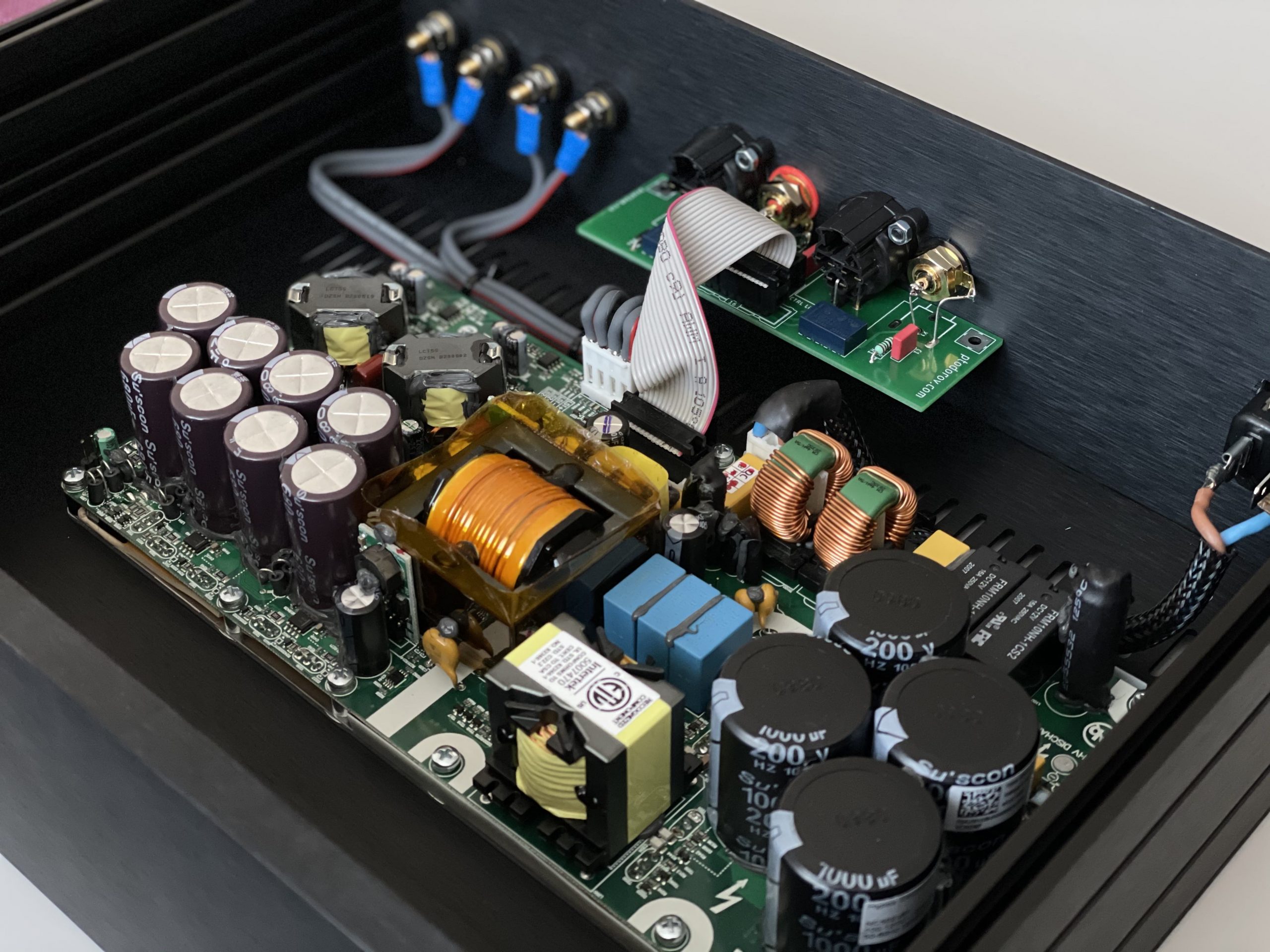
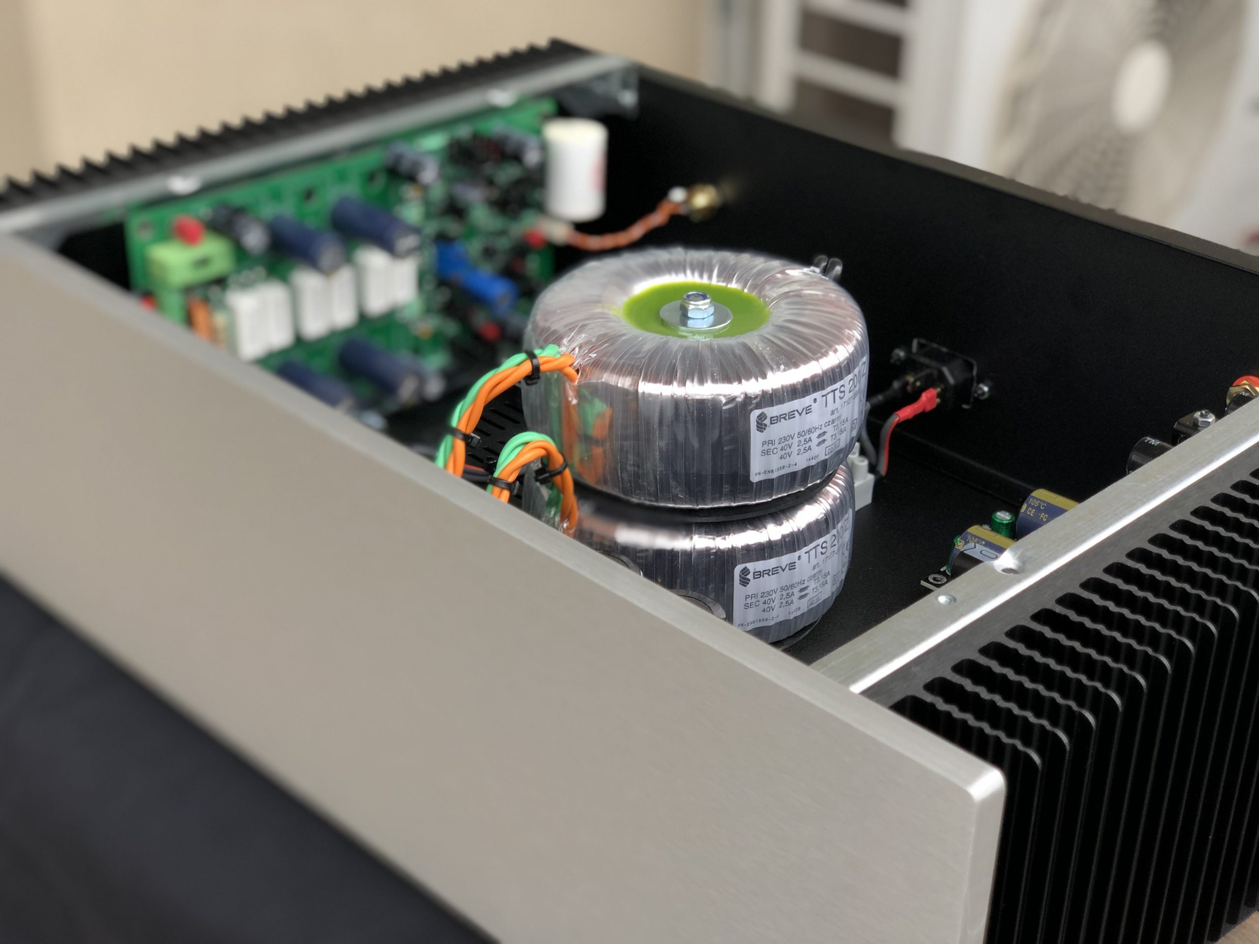
Four separate transformer windings with 3 bridge rectifiers (MCU+LCD; digital section PSU; analog section PSU)
Five on board regulators (LM7805 for the uC/LCD, LT1968-3.3V for the AK4118 and PCM1794 digital supply, LM317(5V) for the PCM1794 analog VCC, LM317/337(+-15V) for the opamp supply.
Ground planes


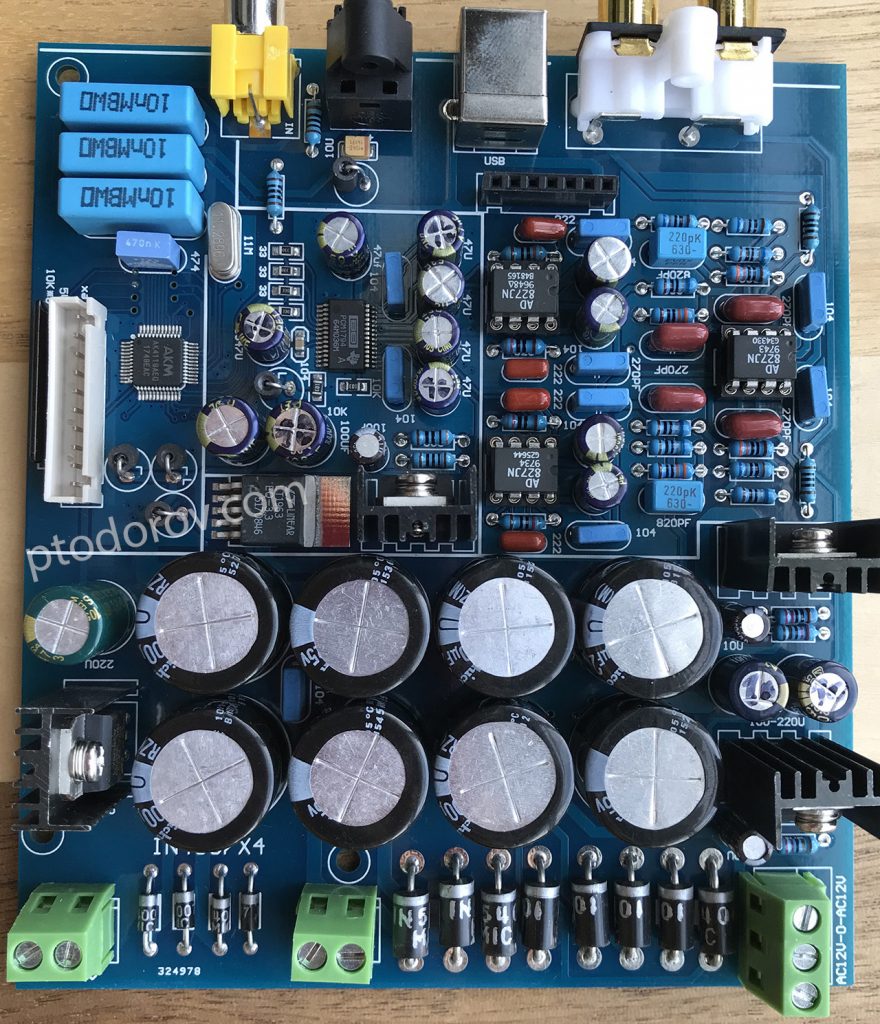
The board costs only 47$ so I expected cheap capacitors and probably fake AD827 opamps. After 20 days I received the board. I was right, they used cheap caps(except the big filter Nichicons, which seem good) and the opamps are probably fake at this price so I started planning mods to the board.

The first thing I did was to test the board before doing anything so I know if it works as expected. I plugged in all required windings, plugged my set-top box as digital source with an optical cable and flipped the switch…

F*ck… The thing is not even working…

Chinese PCM1794 AK4118 board

The first thing I did was to measure all the supplies. I found out that the LT1968-3.3 had 2.0V at its output so the AK4118/PCM1794 didn’t get enough voltage to work. I desoldered the LT1968 and soldered a LD1117V33. It finally worked. Good thing is I don’t have to return it to the seller and I can start with the mods.

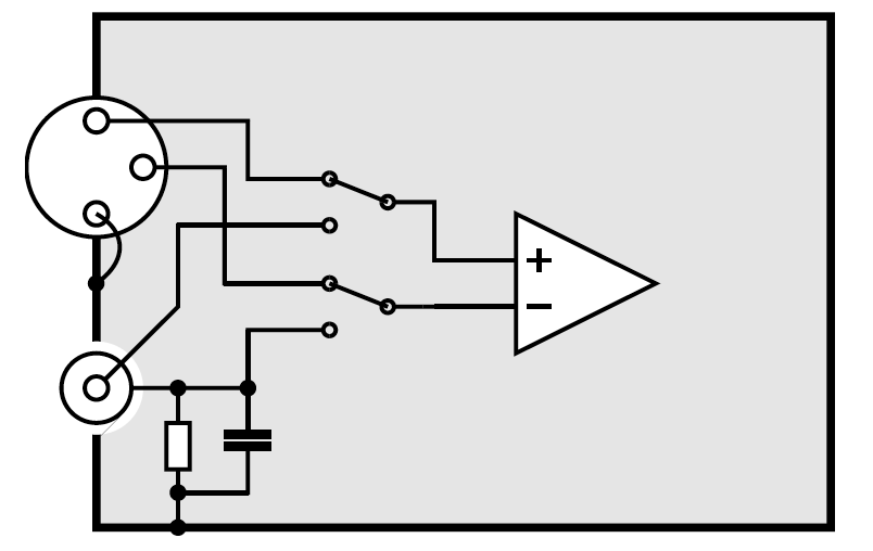
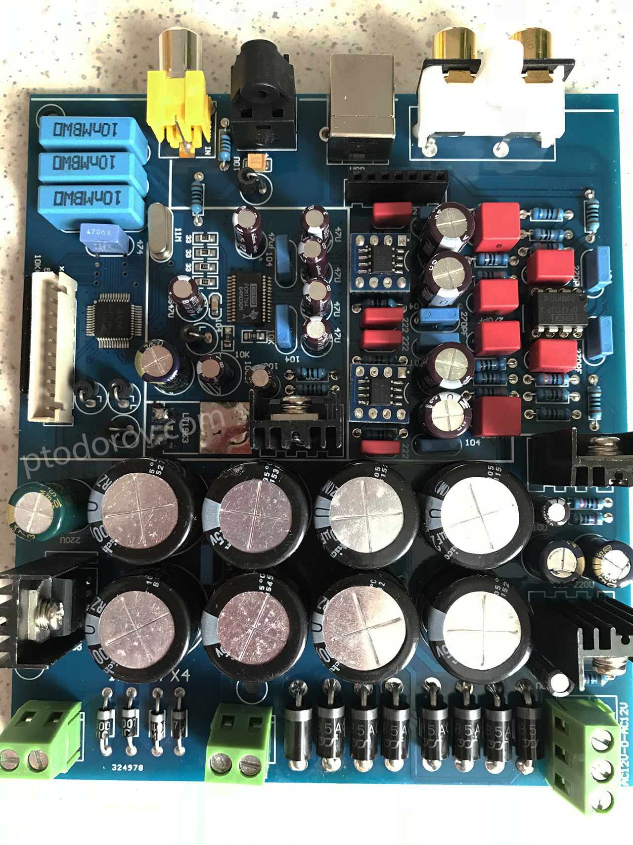
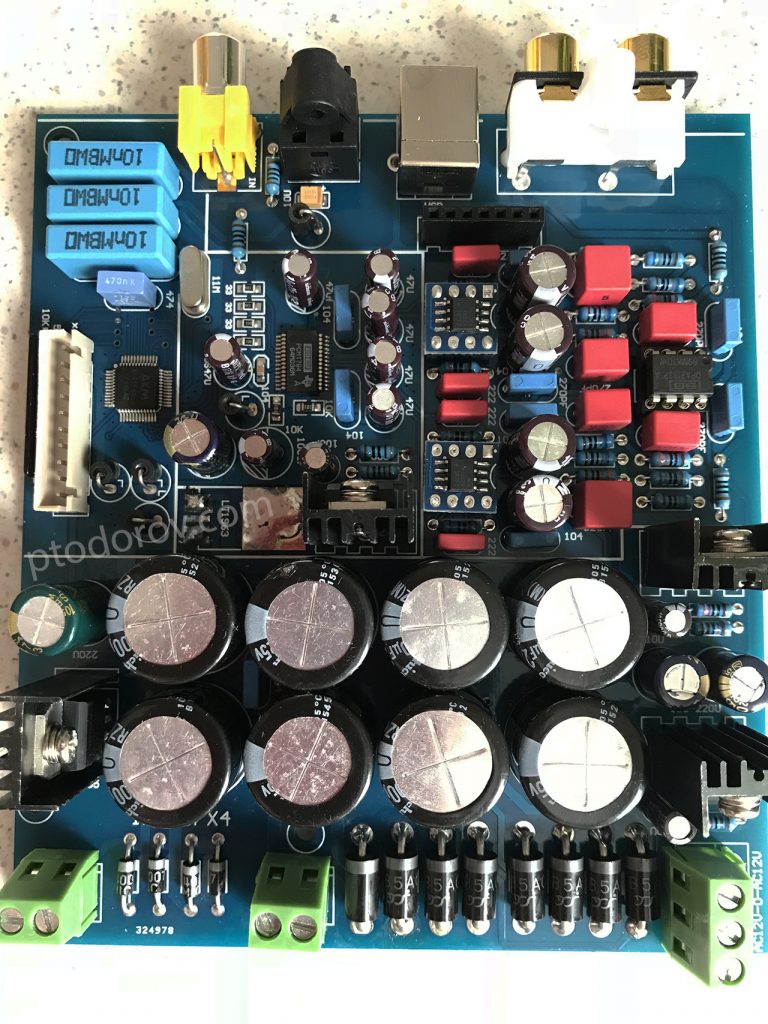
After inspecting the board and following some traces I have annotated the photo of the board of all planned mods for convenience.

PCM1794 DAC planned mods

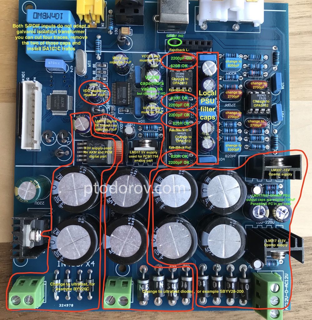
I have done the following modifications:

1. Change all big diodes in the rectifier bridge to SB5A0 fast recovery diodes because the old ones were standard Chinese diodes with shady letters on them.

2. I checked all resistor values according to the following OPA1611(single version of OPA1612) schematic and found out that the 8200pF capacitors were actually 220pF(marked on board as 820pF) and the 2700pF were actually 270pF(marked on board as 270pF). Resistor values were right according to this schematic.
OPA1612 as I/V converter
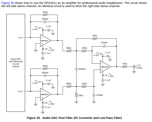
Changed those to Wima FKS2 capacitors with the right values and also changed the 2200pF metallized film capacitors in the feedback of the I/V stage with same value Wima FKS2.

3. Changed all electrolytic capacitors to Nichicon UPS which are low impedance, high temp range capacitors suitable for PSU usage. Some of the capacitors were 47uF instead of the 10uF according to the PCM1794 datasheet.

4. The final thing to do was change two of the AD827(probably fake) to two OPA1612 opamps in the I/V stage and change the third AD827 in the differential to single convertor stage to OPA2132.

PCM1794 AK4118 OPA1612 OPA2132 DAC

I will now let the DAC burn in for a couple dozen hours and I will start listening!

15.01.2019 UPDATE:

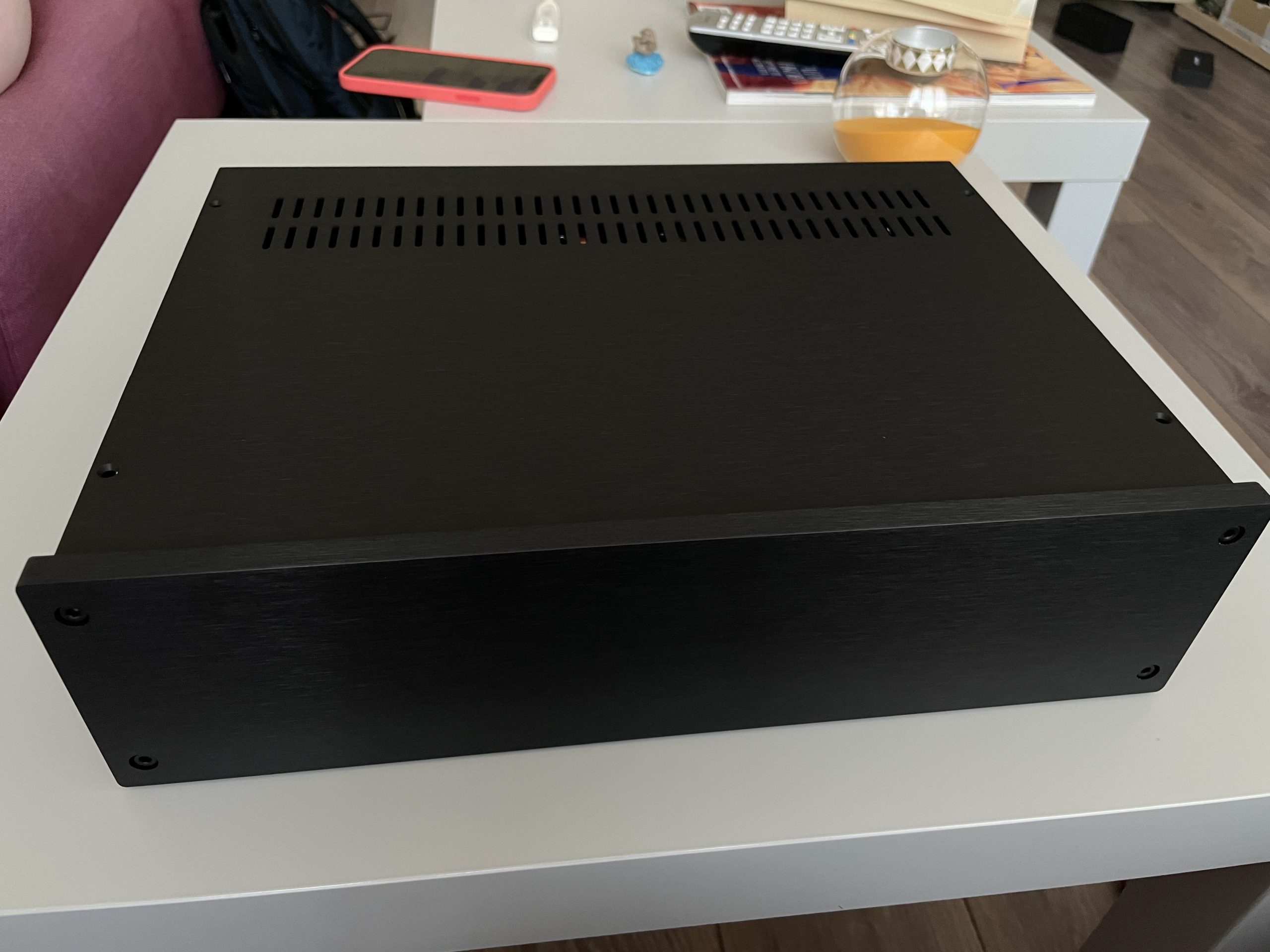
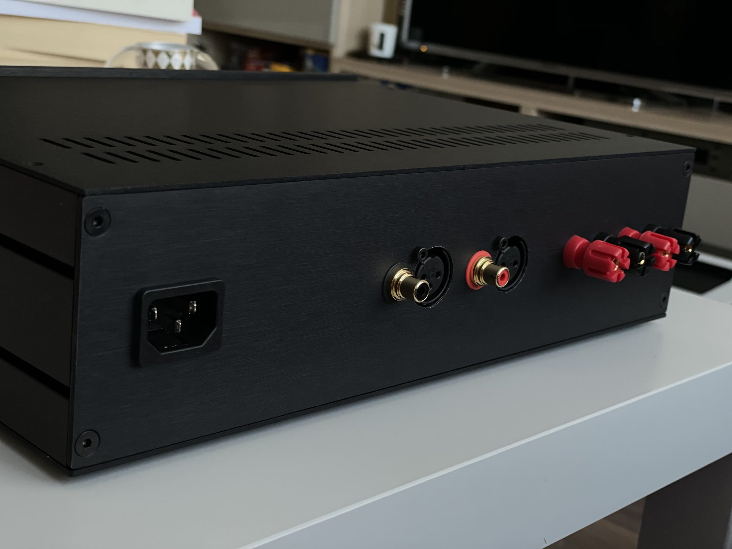
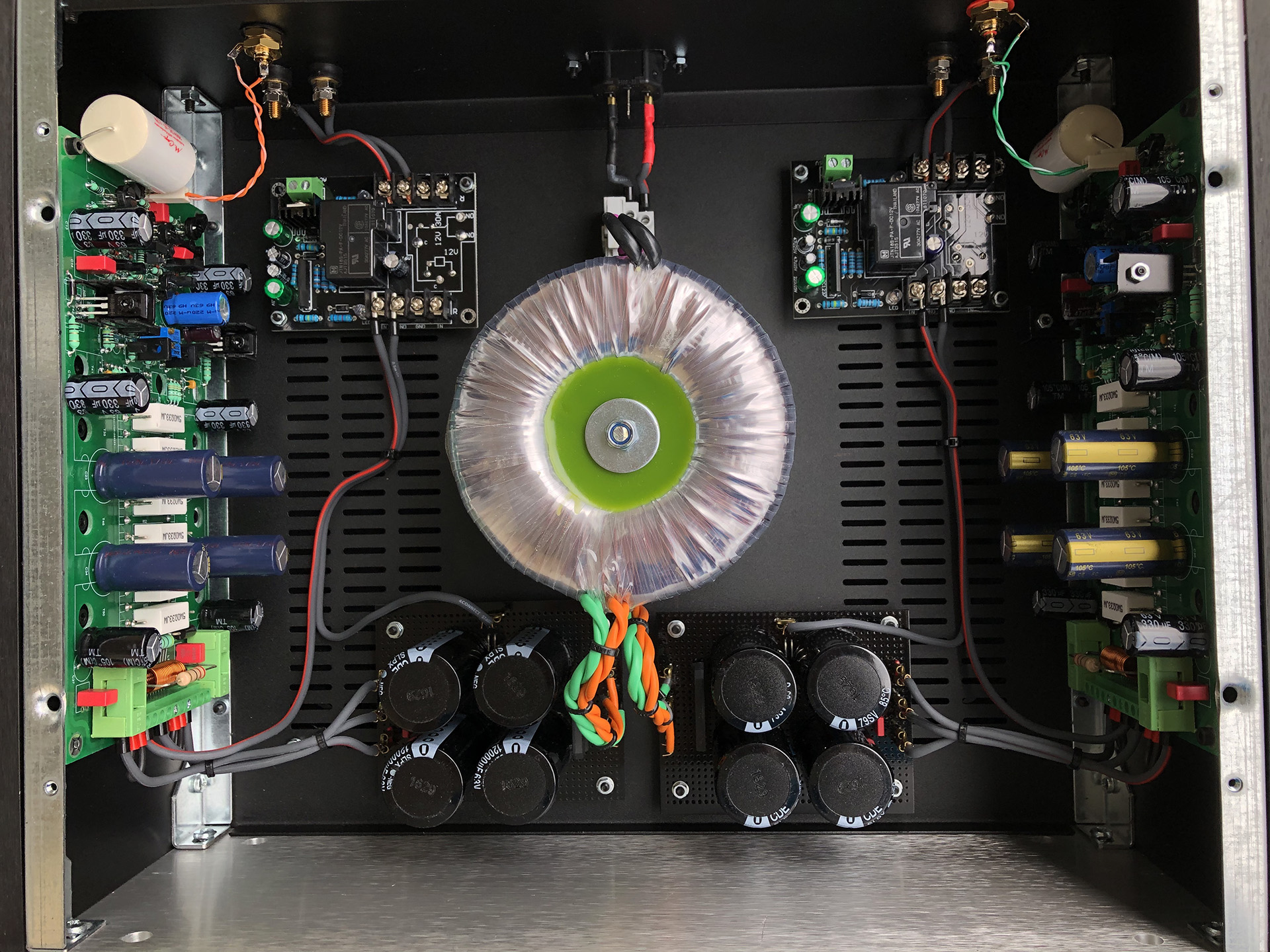
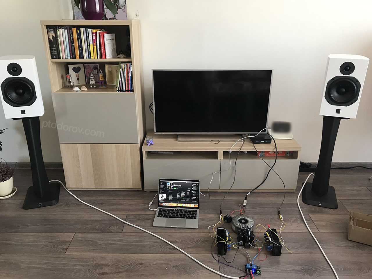
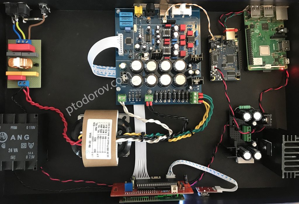
Below is a picture of the full setup in a temporary enclosure consisting of the following:
– A DIY AC filter
– 2x15VAC+2x9VAC R-Core transformer feeding the DAC board
– 2×7,5VAC feeding the XMOS reclock and Raspberry Pi
– Raspberry Pi 3 running Volumio fed by a LT1083 + CRC filter PSU(on the black prototype PCB)
– JLSounds XMOS, with it’s reclock fed by an LM317 + CRC PSU(also on the black board)
– The modified chinese PCM1794 board
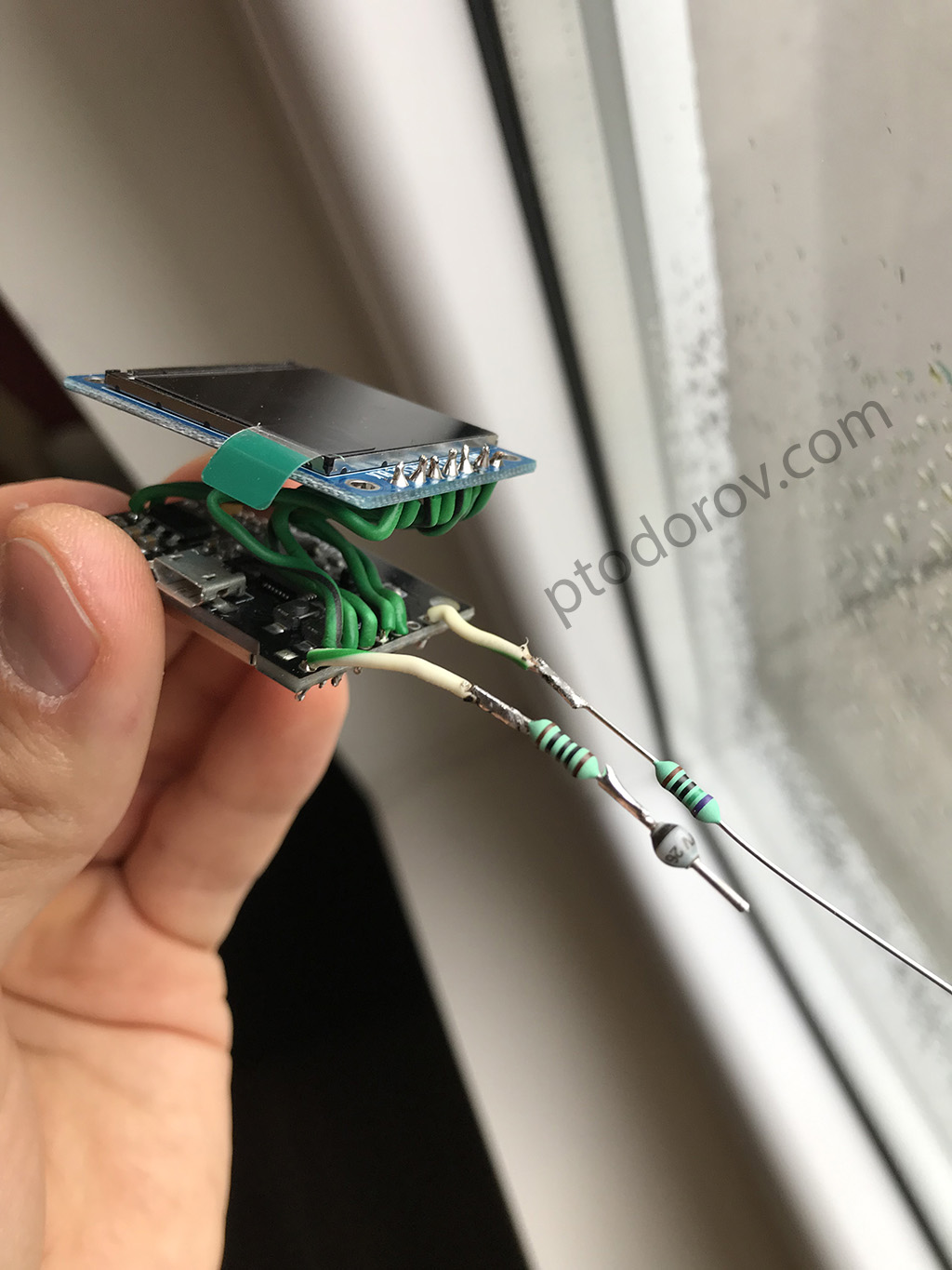
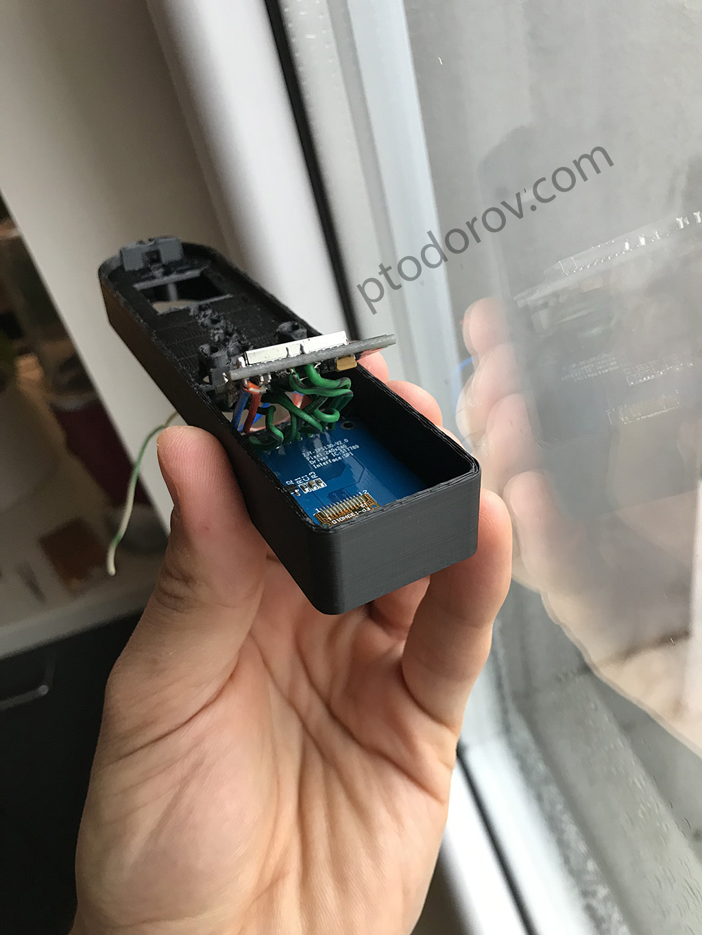
– An LCD display+MCU+rotary switch that came with the Chinese board used to switch digital inputs and display current signal frequency, considering to remove that and put a white on black OLED connected to the Raspberry to display current song, bitrate, res etc.

While still burning in, the sound of the PCM1794 is amazing. TBH I have never expected such a detailed sound that is still warm and pleasant to listen to from a delta-sigma DAC except for the most expensive Sabre pros. I don’t believe the TDA1541 myths anymore.

The good thing is that the whole streamer/DAC costed less than 250$ including the trafos, raspberry, xmos, memory card, DAC board and all the components for the upgrade. It allows me to listen to music from online streaming services such as Spotify and Tidal, USB SSD and I can still switch to the toslink coming from my TV with one click and use the DAC for Xbox(pass-through) and Netflix.

raspberry volumio xmos pcm1794

I will make a full blog post about the whole streamer/DAC once I am done with lower noise discrete PSUs and the enclosure.

UPDATE 10.02.2019:

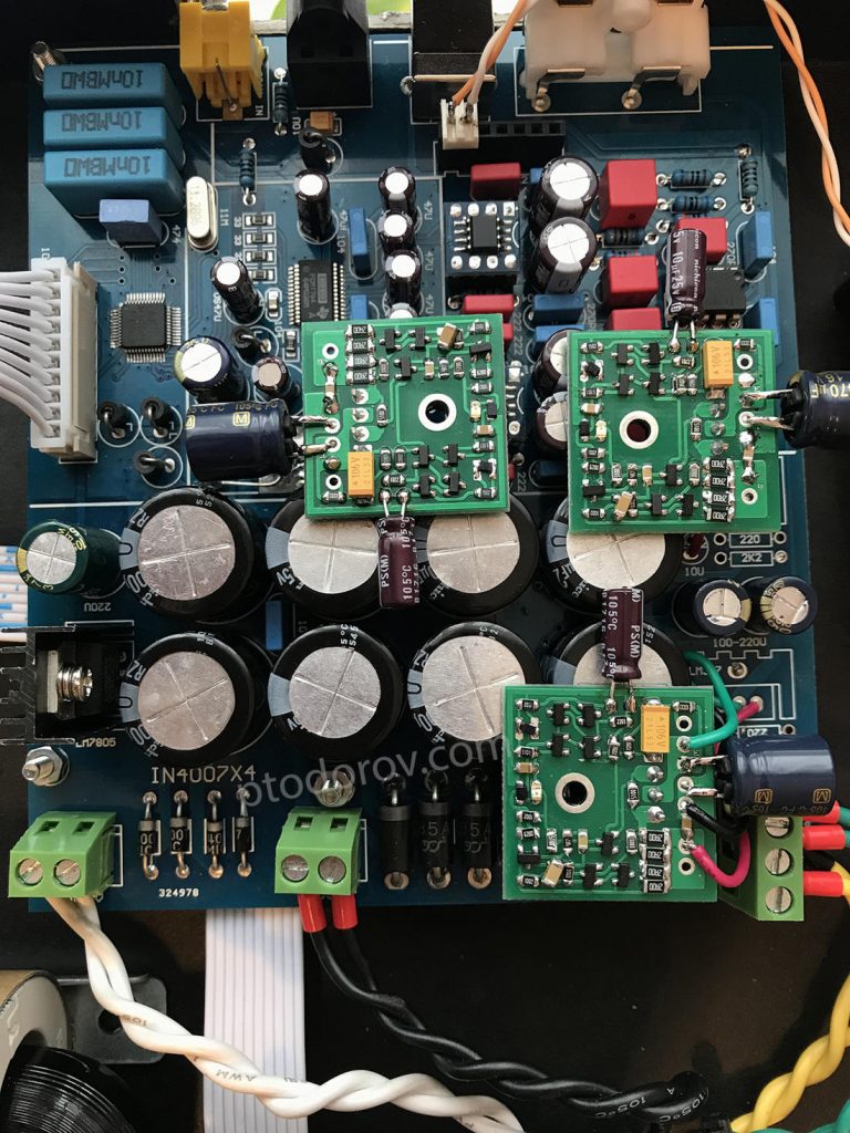
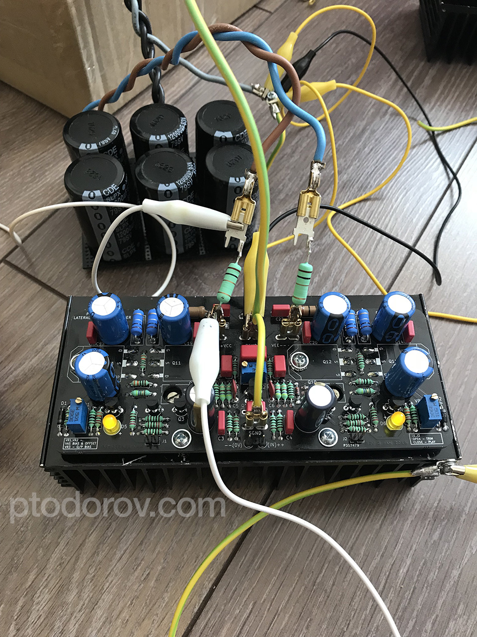
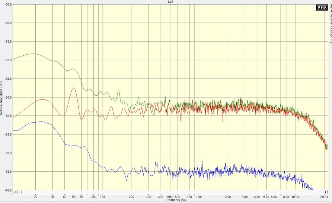
As a final update to the DAC board I decided to replace all the analog audio power supply LM317/337 regulators (opamp supplies and PCM1794 AVCC supply) with DIY discrete regulators with very high Power Supply Rejection Ratio and very low outpud impedance in the audio spectrum. The schematic is designed by a friend from our local audiophile forum (Thanks, Sandy!). Some measurements of the discrete regulator:

The red line is the noise of the discrete regulator, the blue line is the self noise of the measurement setup. WARNING: The numbers are offset by 100dB because of the measurement setup, so -30db must be read as -130dB:
Discrete regulator measurements

So the PSRR of the discrete regulator is ~ -125dB.

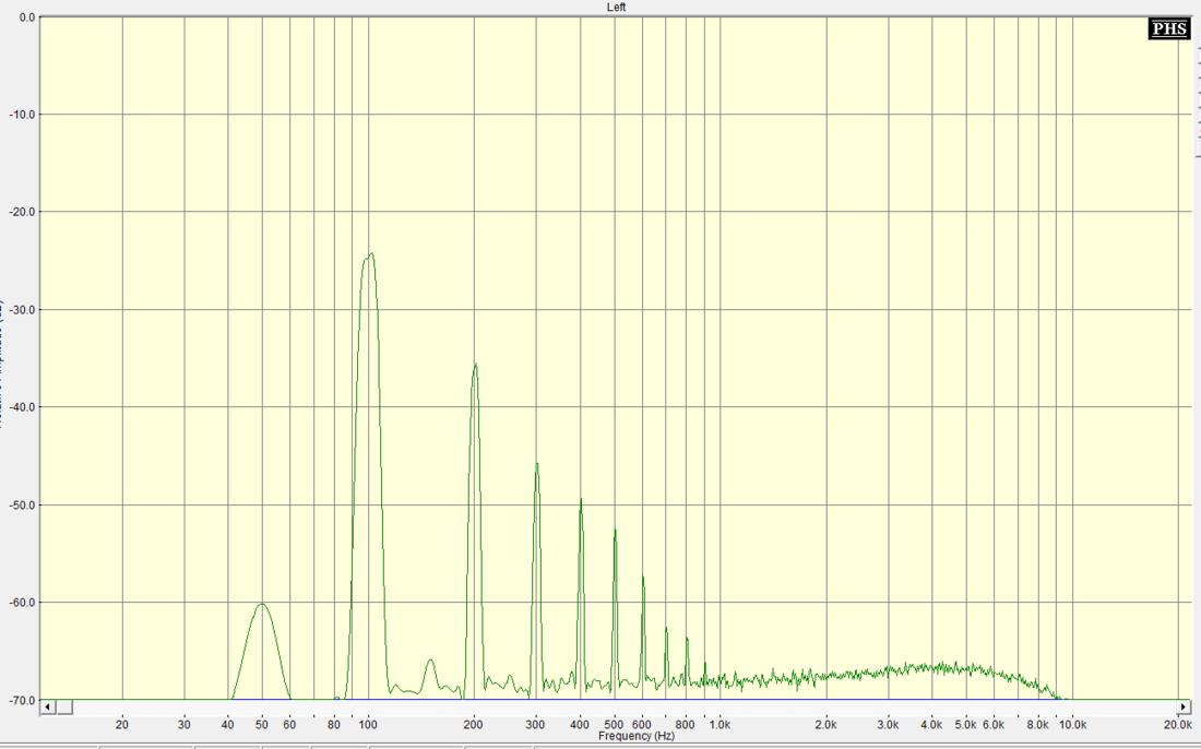
For comparison, measurements of the previous regulators (LM317). WARNING: The numbers are offset by 60dB because of the measurement setup, so -20db must be read as -80dB:

LM317 PSRR measurements
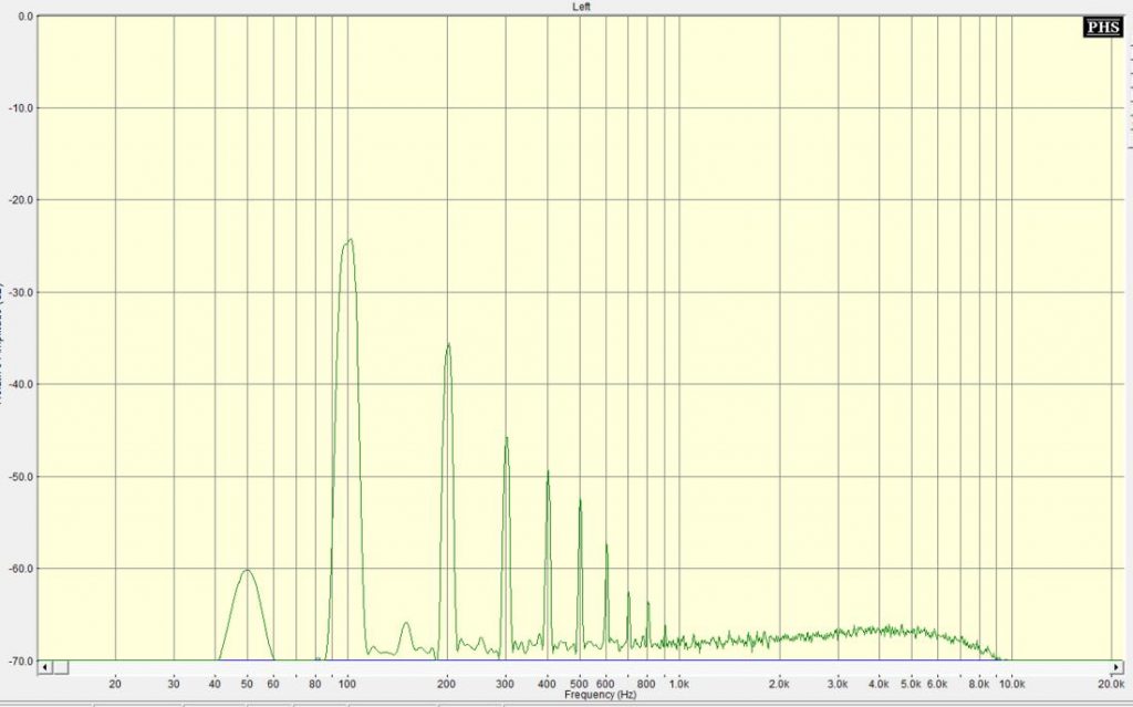
LM317 measured PSRR: ~ -83dB

Also, the discrete regulator has a lot better reaction to load impulses compared to the LM317/337.

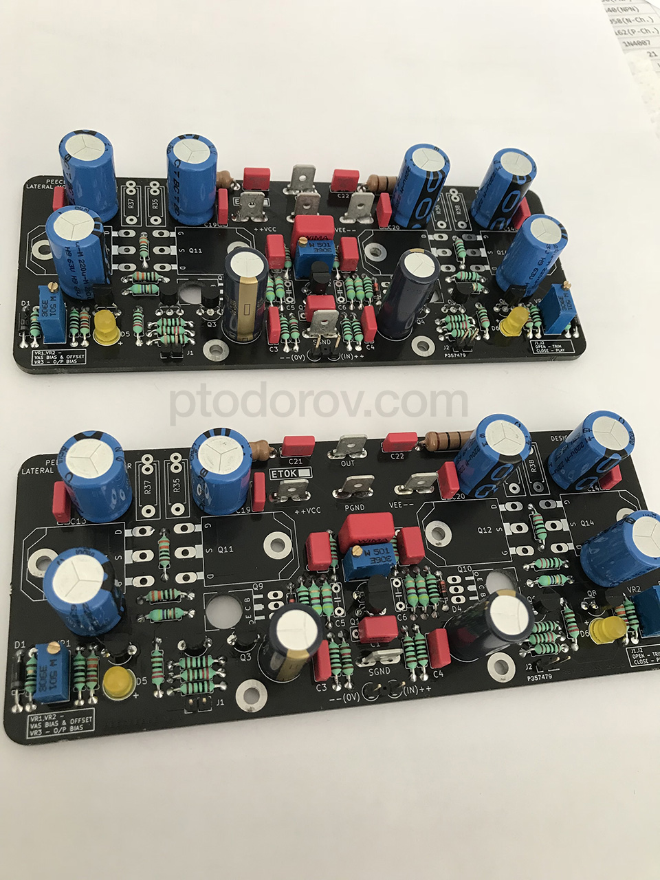
I hate soldering SMD to such tiny boards with my not so good soldering iron but the end result is worth it. A photo with the all three discrete regulators soldered and fit to the board:
PCM1794 Discrete Regulators Fitted

20
Jul

DIY Silver Plated OFC Shielded Interconnects

Today I will be sharing with you a quick guide for a very high quality DIY interconnects at a reasonable price consisting of a silver plated OFC shielded cable from Schutz Kabel and gold plated RCA plugs from Amphenol.

Cable: Schulz Kabel SL 1 – 2m (6.5ft) (official website / my supplier)
– Core: 64×0.1mm silver plated single copper cores
– Shield: 120×0.1mm silver plated single copper cores
– Outer insulation: PVC with natural rubber
– Middle insulation: Thermoplastic elastomer
– Core insulation: Polyethylene
– Costs only 3.68EUR per m

RCA Plugs: Amphenol ACPR-* – 4pcs (official website / my supplier)

– Maximum Cable Diameter: 7mm
– Solid build, long lasting
– Gold plated contacts
– Easy to solder
– Costs only 2.5EUR each

Total cost: 17.36EUR

Note: If you choose to use another RCA plugs or cable make sure that the outside diameter of the cable is not bigger than the RCAs’ maximum cable diameter otherwise you may find it impossible to fit and fix it in the RCA. For example, the Schulz Kabel SL 1 has an outside diameter of 6.5mm and cannot fit in the popular Rean NYS373 RCA plugs which I found the hard way 🙂

(click to enlarge)
DIY Silver plated OFC Interconnects

30
May

Playstation 3 NAND Downgrade guide ( CECHC04 / COK-002 , Teensy 2.0++)

After searching for some time on the Internet on how to downgrade a 60GB PS3 with the COK-002 board, I couldn’t find a guide which explains which testpoint on the COK-002 that is in my PS3 corresponds to the appropriate NAND chip leg. The only thing I could find is that I can use a NAND CLIP to read/write the NANDs but I didn’t feel like giving 60$ and waiting 15 days for a NAND clip that I will use only once.

There are 2 images I found showing which testpoint corresponds to every pin of the Progskeet v1.2 board and the same image for the Infectus board, but I could not find such an image for the Teensy++ 2.0, so I used the image for the Progskeet, along with an image of which Progskeet pin(GP1 etc.) corresponds to which NAND chip pin name (WP, ALE, CLE, I/O1 etc.) to create a diagram of which testpoint on the mainboard goes to which leg of the NAND chips made by Samsung.

PS3 NAND COK Connections

CLICK ON THE IMAGE FOR BETTER RESOLUTION

So now you can use this diagram not only for downgrading/dumping/writing the NANDs with a Teensy++ 2.0 board, but with any other board available on the Internet.

Important!

You must provide a stable 3.3V PSU to both the PS3 board and the Teensy, and don’t forget to unite the GNDs. You can use any PSU which outputs 3.3V @ 1.8A+, the easiest option will be to use a PC PSU.

Short list of the downgrading procedure:

  1. Prepare your Teensy++ 2.0 by using the teensy_loader applications to flash the NANDway .hex file into it
  2. Install Python for Windows and PYserial
  3. Find out which COM port does the new Teensy NANDway use by opening the Device Manager and looking into the Ports(COM&LPT) category
  4. Take apart your PS3 using one of the million videos online for reference
  5. Very carefully solder all the wires according to the diagram above
  6. Solder the other end of all the wires to the teensy board
  7. Find a 3.3V 1.8A+ PSU and solder it to the PS3 mainboard(see the diagram) and to the Teensy++ 2.0
  8. Solder the Teensy++ 2.0 GND to the PS3 mainboard GND
  9. Now on your PC, with the PSU on, the USB cable connected to the Teensy++ 2.0 board run the NANDway python script by issuing the following command in CMD: “NANDway.py COM4”, where COM4 will be the port number you seen in the Device Manager.
  10. You’re done 🙂

Tools used to dump/downgrade/write the NAND chips:

Teensy++ 2.0

NANDway. Now united with NORway in the same repo.

Useful information on the Teensy++ 2.0 PS3 topic here.